From 2nd to 6th Dec, 2017, Prof. Xu Yang of the ISEE college made a report on the recent advancement on High performance ultraviolet and infrared silicon-based photo-detector, on the IEDM conference, San Francisco, the US. Together with the ZJU-UIUC joint college, National key laboratory of the silicon materials, Tsinghua University and the technological physics research institution of the Chinese Academy of Sciences, Prof. Xu made great progress in direction of image sensors during the cooperation. His works, ‘High-Performance, Flexible Graphene/Ultra-thin Silicon Ultra-Violet Image Sensor’ and ‘Graphene/Silicon-Quantum-Dots/Si Schottky-PN Cascade Hetero-junction for Short-Wavelength Infrared Photo-detection’, are both published in the 2017 IEEE IEDM. The news site IEEE Spectrum reported the former paper, and Prof. XU is also shortlisted as a committee member of the 2018 IEEE Electron Devices Technology and Manufacturing Conference committee.
 |  |
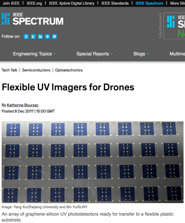 | 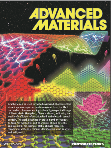 |
Fig01. members of the group of Prof. Xu making report on the IEDM, 2017. The news site IEEEW Spectrum made a special report on the work of Xu: (https://spectrum.ieee.org/tech-talk/semiconductors/optoelectronics/flexible-uv-imagers-for-drones). His previous work on the photo-detectors was used as the inside cover for Advance Materials.
‘Modern ultraviolet (UV) photo-detection demands high performance with additional feature such as flexibility. While wide-band-gap (WBG) based semiconductors have emerged as the most recent technological solutions for high performance UV photo-detection, the issues, such as low crystal quality and lack of flexibility, hinder their wide-spread applications. Though Silicon (Si) offers several advantages over WBG semiconductors, such as low-density surface states, high reliability, matured manufacturing, and high-speed detection, one significant disadvantage of Si photo-diodes is the inherent broadband response (extending form X-rays to near infrared), which in the first place led to the development of WBG semiconductor based photo-detectors. Penetration depth of light in Si falls sharply with decreasing wavelength. For example, UV light with λ<360 nm has a shallow penetration depth of only 20 nm. We envision that by thinning bulk silicon down to the length scale of penetration depth of UV would not only significantly reduce the absorption of longer wavelengths (visible and IR), but also provide mechanical flexibility lacked in Si-based devices.’[1]
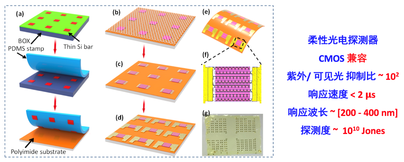
Fig2.(a) transferring ultra thin Si to flexible PI substrate with the help of PDMS; (b-f) device manufacturing process; (g) device array on the PI substrate
‘Due to limited short-wavelength infrared (SWIR) (1.1-2.5 μm) response of silicon (Si), germanium and indium-gallium-arsenide based photo-detectors have dominated the commercial market of SWIR photo-detectors for decades. However, they are often constrained by high-temperature processing, spectral range, flexible incompatibility, and cryogenic cooling accessories. Therefore, it is important to develop photo-detectors that can be directly integrated with complementary-metal-oxide-semiconductor devices. In this work, we demonstrate a Si-based SWIR photo-detector operating in the wavelength range from 800 to 1870 nm, with responsibility up to 0.6 A/W, and operation speed down to 15 p, s. By taking advantage of the fast photo-carriers transfer between graphene (Gr) and Si-quantum-dots (QDs), along with SWIR tunable Schottky-barrier height of Gr-Si junction, a novel Schottky-PN cascade hetero-junction based photo-detector has been demonstrated. The hyper-boron-doped SiQDs, interacting with the Gr-Si Schottky photo-diode, effectively and fast harvest SWIR-excited charge-carriers. The cascade photo-diode working at room temperature, with detectivity of 1011 Jones and sensitivity of 10-13 W/Hz05, manifests a promising prospect of our Si-based SWIR photo-detector.’ [2]
The group has been devoted to combing two dimensional materials and the silicon-based photo-detectors, the so-called ‘Si+2D’ strategy. A series of outcomes have been produced and published on the Nature Communications, Advanced Materials and ACS Nano, providing new paths for future exploration of the Si-based photo-detectors.
All these works are conducted under the support and funding of the NSFC (61674127, 61474099), ZJ-NSF (LZ17F040001), Zhejiang advanced micro-nano electronic devices intelligence systems and applications key laboratory, ZJU-UIUC joint college and the National Silicon Materials Key Laboratory.
The cross-section research has received the generous help from professor Yu Bin, Li Erping, Chen Hongsheng, Yang Jianyi, Luo Jikui, Yin Wenyan, Yang Deren and their teams during progress. The help has been great in the fields listed: device structural capacitance and resistance optimization by Cheng Zhiyuan, Yang Dongxiao, Dong Shurong, Li Yubo; flexible devices and performance analyze by Chen Weiqiu, Qu Shaoxing, Song Jidan; high quality graphite & Si-Schottky knot craft wafer by Dai Daoxin, Zhu Dazhong, Wang Xi; making and high quality transferring of CVD single-crystal graphite by Wang Hongtao, Zhao Pei; quantum point synthesize and representation by Pi Xiaodong, Peng Xiaogang; ALD atom sediment by Zhou Qiang; graphite plasma erosion by Lin Shisheng; thin film sputtering by Ye Zhi, Jin Hao; high quality SiN and SiO2 PECVD thin film sediment by Zhao Yi, Liu Yang; high distinguishability electron microscope using HRTEM and SEM by Jin Chuanhong, Wang Yong; electron cluster erosion by Qiu Min, Li Qiang; FTIR by Fan Xianping, Qiao Xusheng; Raman representation by Tan Pingheng; KPFM surface work function analyze by Jin Yizheng; DLTS flaw state deep energy level analyze by Yu Xuegong, Ma Xiangyang; pico second laser pulse light path design by Ruan Zhichao, Wu Xidong, Hao Ran; GHz high speed photo-electronic test and chopper modulation by Jin Xiaofeng, Zhang Xianmin, Yu Hui, Jiang Xiaoqing, Li Yubo; STM representation analyze, UV vs. NIR and phase-lock amplifier by Xie Jin; low temperature test and photo-electronic detector array chips packing by Zhu Dazhong; peripheral low-frequency filtering and low noise multiple resistance amplification circuit test by Han Yan, Zhao Yi, Wang Xiaozhi, Yu Xiaopeng.
[1] A. Ali, K. Shehzad, H. Guo, Z. Wang, P. Wang, A. Qadir, W. Hu, T. Ren, B. Yu and Yang Xu*, “High-Performance, Flexible Graphene/Ultra-thin Silicon Ultra-Violet Image Sensor”, IEDM 8.6, 2017.
[2] S. Du, Z. Ni, X. Liu, H. Guo, A. Ali, Yang Xu* and Xiaodong Pi*, “Graphene/Silicon-Quantum-Dots/Si Schottky-PN Cascade Heterojunction for Short-Wavelength Infrared Photodetection”, IEDM 8.7, 2017.
[3] X. Wan, Yang Xu*, H. Guo, K. Shehzad, A. Ali, Y. Liu, J. Yang, D. Dai, C.-T. Lin, L. Liu, H.-C. Cheng, F. Wang, X. Wang, H. Lu, W. Hu, X. Pi, Y. Dan, J. Luo, T. Hasan, X. Duan, X. Li, J. Xu, D. Yang, T. Ren and B. Yu, "A self-powered high-performance graphene/silicon ultraviolet photodetector with ultra-shallow junction: breaking the limit of silicon?" npj 2D Materials and Applications 1(1): 4, 2017.
[4] T. Yu, F. Wang, Yang Xu*, L. Ma, Xiaodong Pi*, Deren Yang*, "Graphene Coupled with Silicon Quantum Dots for High-Performance Bulk-Silicon-Based Schottky-Junction Photodetectors." Advanced Materials 28(24): 4912-4919, 2016.
[5] Z. Ni, L. Ma, S. Du, Yang Xu*, M. Yuan, H. Fang, Z. Wang, M. Xu, D. Li, J. Yang, W. Hu, Xiaodong Pi* and Deren Yang*, "Plasmonic Silicon Quantum Dots Enabled High-Sensitivity Ultrabroadband Photodetection of Graphene-Based Hybrid Phototransistors." ACS Nano 11(10): 9854-9862, 2017.
[6] G. Hu, T. Albrow-Owen, X. Jin, A. Ali, Y. Hu, R. C. T. Howe, K. Shehzad, Z. Yang, X. Zhu, R. I. Woodward, T.-C. Wu, H. Jussila, J.-B. Wu, P. Peng, P.-H. Tan, Z. Sun, E. J. R. Kelleher, Meng Zhang*, Yang Xu* and Tawfique Hasan*, "Black phosphorus ink formulation for inkjet printing of optoelectronics and photonics." Nature Communications 8(1): 278, 2017.
[7] S. Du, W. Lu, A. Ali, P. Zhao, K. Shehzad, H. Guo, L. Ma, X. Liu, X. Pi, P. Wang, H. Fang, Z. Xu, C. Gao, Y. Dan, P. Tan, H. Wang, C.-T. Lin, J. Yang, S. Dong, Z. Cheng, E. Li, W. Yin, J. Luo, Bin Yu, T. Hasan, Yang Xu*, Weida Hu* and X. Duan, "A Broadband Fluorographene Photodetector." Advanced Materials 29(22): 1700463, 2017.
[8] Yang Xu*, A. Ali, K. Shehzad, N. Meng, M. Xu, Y. Zhang, X. Wang, C. Jin, H. Wang, Y. Guo, Z. Yang, B. Yu, Y. Liu, Q. He, X. Duan, X. Wang, P.-H. Tan, W. Hu, H. Lu and Tawfique Hasan*, "Solvent-Based Soft-Patterning of Graphene Lateral Heterostructures for Broadband High-Speed Metal–Semiconductor–Metal Photodetectors." Advanced Materials Technologies 2(2): 1600241, 2017.
[9] K. Shehzad, T. Shi, A. Qadir, X. Wan, H. Guo, A. Ali, W. Xuan, H. Xu, Z. Gu, X. Peng, J. Xie, L. Sun, Q. He, Z. Xu, C. Gao, Y.-S. Rim, Y. Dan, T. Hasan, P. Tan, E. Li, W. Yin, Z. Cheng, B. Yu, Yang Xu*, J. Luo and X. Duan, "Designing an Efficient Multimode Environmental Sensor Based on Graphene–Silicon Heterojunction." Advanced Materials Technologies: 1600262, 2017.
[10] S. Chen, X. Liu, X. Qiao, X. Wan, K. Shehzad, X. Zhang, Yang Xu* and Xianping Fan*, "Facile Synthesis of γ-In2Se3 Nanoflowers toward High Performance Self-Powered Broadband γ-In2Se3/Si Heterojunction Photodiode." Small 1604033, 2017.
[11] K. Shehzad, Yang Xu*, C. Gao and X. Duan, "Three-dimensional macro-structures of two-dimensional nanomaterials." Chemical Society Reviews 45(20): 5541-5588, 2016.
[12] Yang Xu*, C. Cheng, S. Du, J. Yang, B. Yu, J. Luo, W. Yin, E. Li, S. Dong, P. Ye and X. Duan, "Contacts between Two- and Three-Dimensional Materials: Ohmic, Schottky, and p–n Heterojunctions." ACS Nano 10(5): 4895-4919, 2016.
[13] Kuei-Lin Chiu* and Yang Xu*, "Single-electron transport in graphene-like nanostructures." Physics Reports 669: 1-42, 2017.
