01 Research Background
Si Photonic Integrated Circuits, with advantages of small size, low coupling and large bandwidth, has become an increasingly advanced technology that meets the demands of big data transmission. Transferring optical signals to electrical signals, waveguide-integrated photodetector is an important component in silicon photonic circuits that connects silicon photonic platforms and silicon electronic platforms. Currently, the commercial band-integrated detectors are mainly based on the integration of Ge, Si waveguides and III-V semiconductors. Subject to the differences of parameters including lattice constant and coefficient of thermal expansion, growing photosensitive materials onto Si platforms has met barriers of expense and monolithic integration.
In recent years, two-dimensional materials have gradually shown their advantages in waveguide-integrated photodetectors. Firstly, combined with Van der Waals force, two-dimensional materials have integration capability without lattice matching requirements, integrating perfectly with silicon-based platforms and therefore meets the requirements of large-scale integrated device fabrication. Secondly, two-dimensional materials possess an ultrahigh carrier mobility (e.g. 2×10^5 cm^2/(V·s) for graphene). Besides, two-dimensional materials have other excellent characteristics such as high carrier intriguing optical absorption, tunable optoelectronic parameters and excellent optical absorption performance in O-U band.
02 Introduction to the Paper
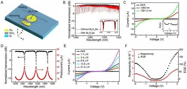
Recently, research group led by Prof. LIN Hongtao of ZJU’s College of Information Science and Electronic Engineering and Dr. LI Lan of Westlake University School of Engineering, together with Dr. LIU Bilu and Dr. XU Xiaomin of Tsinghua Berkeley Shenzhen Institute and Dr. Tang Bo of Institute of Microelectronics of the Chinese Academy of Sciences, jointly reported an integration process of Bi2O2Se with silicon waveguide and silicon-based microring, developing a high-performance O band photodetector. The authors quantitatively characterized the absorption coefficient of the Bi2O2Se/Si hybrid waveguide with unbalanced Mach–Zehnder interferometer (MZI) and the refractive index of Bi2O2Se in O band with microring. The reported photodetector has the characteristics of low dark current, high response, low noise-equivalent power, fast response speed and wide spectral response. In addition, it also presents a wavelength selective detection function. The findings were published on ACS Nano.

The authors synthesized high-quality Bi2O2Se on an f-mica substrate by the chemical vapor deposition (CVD) method, and utilized lithography and ion beam milling to obtain high-performance passive optical devices including optical grating, waveguide, multimode interference and microring resonator. Meanwhile, they succeed in integrating Bi2O2Se with Si waveguide and microring by dry transfer process. All in all, this MRR-enhanced photodetector shows an advantage for optimizing a photodetector, and the wavelength-sensitive characteristics have the potential in a wavelength division multiplexing system for on-chip spectroscopy, sensing, and communication.

Prof. LIN Hongtao's group.
